
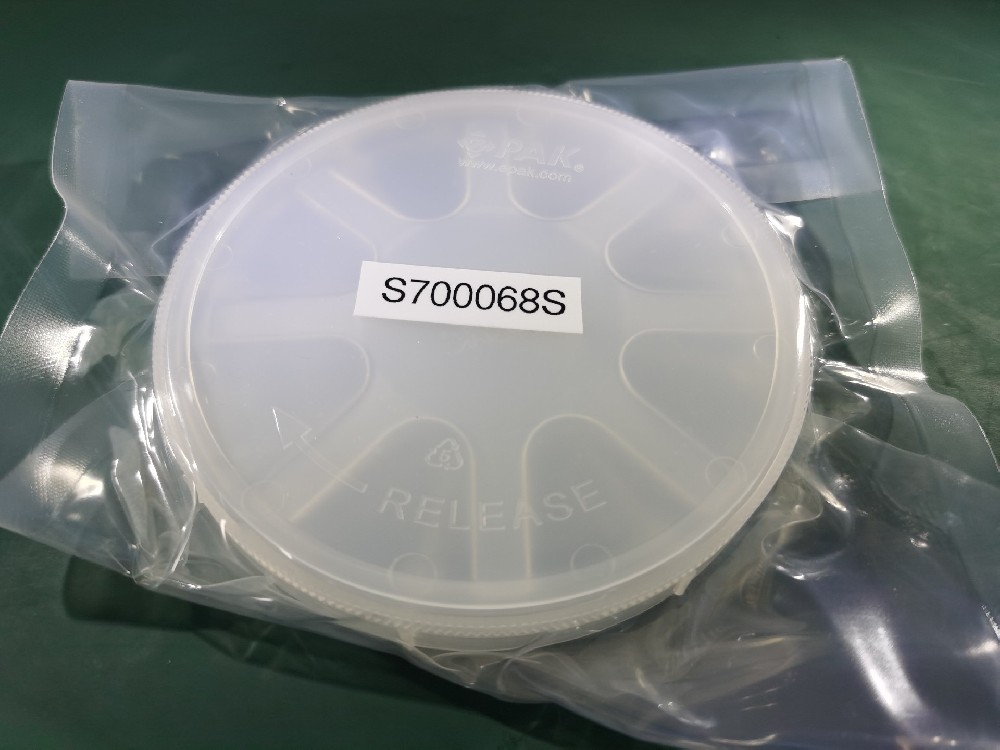
| Product size: | Standard sizes available, custom sizes supported. |
| Product Price: | Inquire Customer Service |
| Packaging Method: | Special individual boxes/single pieces |
| Shipping Methods: | Express delivery, sea freight & international shipping |
| Samples Offered: | Custom sample service is supported. |
Sapphire wafers are monocrystalline substrates crafted from synthetic sapphire,which is a crystalline form of aluminum oxide (Al2O3). These wafers are extensivelyutilized for the epitaxial growth of III-V compounds and serve as the most prevalentstrate material for gallium nitride (GaN) light-emitting diodes (LEDs).
Recommended specification of sapphire wafer
2 inch C plane sapphire wafer 3 inch C plane sapphire wafer 4 inch C plane sapphire wafer6 inch C plane sapphire wafer 8 inch C plane sapphire wafer | A (11-20) plane sapphire wafer R (1-102) plane sapphire wafer M (10-10) plane sapphire wafer | C-A off cut 1° | 2° | 4° | 6° C-M off cut 1° | 2° | 4° | 6° R-M off cut 1° | 2° | 5° | 8° A-M off cut 7° (Substrates for dimond epitaxy) |
* All wafers have options for single sided polish (SSP) and dobule sided polish (DSP). * Customized dimension and thickness as per required is available. * Customized orientation and off-cut angle as per required is available. | ||
Crystal Orientations
C [0001], A [11-20], R [1-102], and M [10-10] are Miller indices for specific crystallographic axes in the hexagonal lattice of monocrystalline sapphire. Together, they define the "C/A/R/M-plane," a characteristic plane where atomic arrangements along these axes form a critical planar structure for the crystal's properties.C-plane sapphire substrates are the predominant epitaxial templates for GaN and LEDs, while nonpolar M-plane and semipolar R/A-plane substrates reduce polarization effects, improve carrier distribution, and boost device efficiency, durability, and stability.
Misoriented (miscut)
A misoriented (miscut) sapphire substrate refers to a sapphire ingot that is intentionally cut at an angle deviating from a specific crystallographic orientation (e.g., the c-axis), creating a stepped surface structure, this stepped morphology enables controlled crystallographic orientation, guiding epitaxial growth or surface treatment directionality. For example, in MoS2 single-crystal growth, step-edge atomic arrangements break energy degeneracy, achieving high-yield unidirectional domain growth. Miscut sapphire substrates are currently utilized for synthesizing two-dimensional materials, diamond, graphene, and other advanced materials.
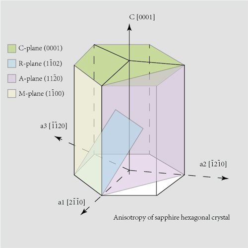
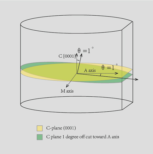
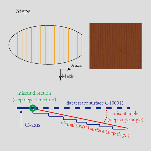
Anisotropy of sapphire hexagonal crystal, off-cut sapphire wafer, stepped surface structure
Surface Processing Technology
Chemical Mechanical Polishing (CMP) achieves nanoscale flatness on wafer surfaces through the synergistic effect of chemical etching and mechanical abrasion. Its principle involves abrasive-laden polishing slurries reacting with the wafer surface to soften the top layer, which is then removed via mechanical friction from the polishing pad, enabling global planarization. Our sapphire wafers utilize aluminum oxide and silicon oxide polishing abrasives with large-scale lapping and polishing equipment, delivering stable surface quality: surface roughness Ra < 0.3 nm, Total Thickness Variation (TTV) < 5 microns, and Bow < 5 microns.
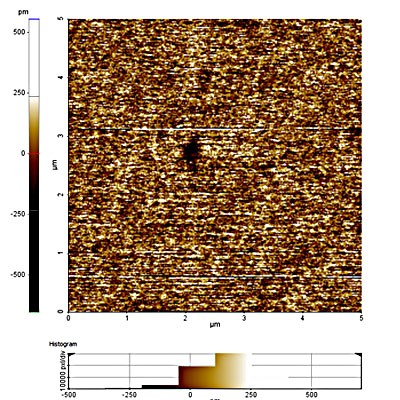
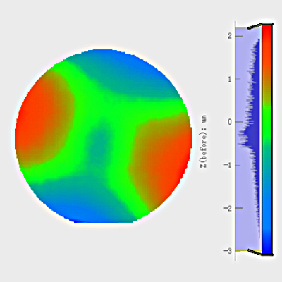
Surface roughness and BOW inspection
SEMI-Compliant Cleaning & Packaging
In semiconductor manufacturing, the cleaning process is critical to device performance, requiring precise control of temperature, pH levels, and chemical formulations. Our sapphire wafers utilize the standard wet cleaning flow "SC3→QDR→SC1→QDR", employing strong acidic and alkaline cleaning solutions in conjunction with deionized water (DIW) for efficient rinsing. This process thoroughly removes organic residues, metal ions, particles, and oxide layers from the wafer surface, achieving global cleanliness. The entire cleaning procedure is conducted in a cleanroom environment to control airborne particulates, and post-cleaning wafers are dried using a spin-drying technique to prevent water marks or re-adhesion of contaminants.
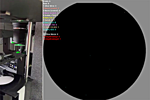
Particles inspection by AOI
Service: wafer Laser dicing
We employ laser cutting technology to customize sapphire wafers in special sizes, achieving ±0.1mm precision and smooth edges. This technique utilizes a high-energy laser beam interacting with sapphire through the photothermal effect to enable precise cuts. It ensures high accuracy, smooth edges, minimal heat impact, and prevents thermal stress damage.
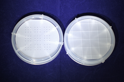
Laser dicing and drilling on sapphire wafers
Relevant product: GaN epitaxy on sapphire
We collaborate with third-party laboratories to provide epitaxial processing services using MOCVD or HVPE equipment. We can grow gallium nitride (GaN) epitaxial layers with thicknesses ranging from 1 to 15 micrometers on sapphire substrates through chemical vapor deposition. This is a complex product, so please contact us to discuss specific epitaxial structures and process requirements.


 English
 中文版
中文版